High Speed Serial Interface (HSSI) Design Specification
Available Languages
Date: April 12, 1993
Revision 3.0
Previous Release:
Revision 2.11
March 16, 1990
First Release: October 1989
Addendum Issue #1: January 1991
Copyright© 1989-1993 by Cisco Systems, Inc. and T3plus Networking, Inc.
Notice
Cisco Systems, Incorporated and T3plus Networking, Incorporated make no representation in respect to and does not warrant any of the information in the Specification, but furnishes such in good faith and to the best of its knowledge and ability. Without restricting the generality of the foregoing, Cisco Systems and T3plus Networking make no representations or warranties as to fitness for a particular purpose, or as to whether or not the use of the information in the Specification may infringe any patent or other rights of any person. The recipient waives any claims it may have against Cisco Systems or T3plus Networking in respect of any use which the recipient makes of the information or products derived therefrom.
Permission is granted to reproduce and distribute this specification provided:
- Cisco Systems, Inc. and T3plus Networking, Inc. names appear as authors,
- a copy of this notice appears on all copies,
- the contents of this document are not altered or modified.
The contents of this document may not be altered or modified without the express written permission of Cisco Systems and T3plus Networking. It is intended that this document will serve as a high speed serial interface Specification and evolve into an industry standard. With this intent, it is expected that this Specification may be revised in the future to reflect additional requirements or adherence to domestic or international standards as they evolve. Cisco Systems and T3plus Networking reserve the right to alter or modify this Specification or the equipment it relates to at any time without notice and without liability.
To receive updated copies of this specification, it is advisable to request that you are added to the HSSI Specification mailing list of either Cisco Systems or T3plus Networking.
Joint Authors
John T. Chapman
Senior Hardware Design Engineer
Cisco Systems, Inc.
375 East Tasman Drive
San Jose, CA 95134
jchapman@cisco.com
TEL: (408) 526-7651 FAX: (408) 527-1709
Mitri Halabi
Senior Hardware Design Engineer
T3plus Networking, Inc.
2840 San Tomas Expressway
Santa Clara, CA 95051
mitri@t3plus.com
TEL: (408) 727-4545 FAX: (408) 727-5151
Introduction
Abstract
This document specifies the physical layer interface that exists between a DTE such as a high speed router or similar data device and a DCE such as a DS3 (44.736 Mbps) or SONET STS-1 (51.84 Mbps) DSU. Future extensions to this specification may include support for rates up to SONET STS-3 (155.52 Mbps).
This document is specification compatible with the HSSI Design Specification, written by John T. Chapman and Mitri Halabi, Revision 2.11, dated March 16, 1990 and Addendum Issue #1, dated January 23, 1991.
HSSI is currently being ratified by the American Standards Intitute. The physical layer specification will be EIA/TIA-613 and the electrical layer specification will be EIA/TIA-612. These specifications should become available in mid 1993. Notation has been included here where there are known differences between the two specifications.
Document Organization
- This section, Introduction, introduces HSSI and relates it to other specifications.
- The next section, Terms and Definitions, provides the definitions used in the document.
- The third section, Electrical Specification, defines the electrical specifications, including signal names, definitions, characteristics, operation, and timing.
- Section four, Physical Specification, describes the physical properties including connector types, cable types, and pin assignments.
- Appendix A, Timing Diagrams, graphically relates timing relationships.
- Appendix B, Differential Circuit Conventions, graphically defines polarity conventions.
- Appendix C, Noise Immunity, has a detailed analysis of ECL noise immunity.
Comparison to Existing Standards
With respect to the ANSI/EIA series of standards, EIA-232-D, EIA-422-A, EIA-423- A, EIA-449, and EIA-530, this specification is distinct in that it:
- supports serial bit rates up to 52 Mbps
- uses emitter coupled logic (ECL) transmission levels
- allows the timing signals to be gapped, i.e., discontinuous
- uses a simplified control signal protocol
- uses a more detailed loopback signal protocol
- uses a different connector
Terms and Definitions
This specification adheres to the following definitions:
-
Analog Loopback
-
A loopback in either direction that is associated with the line side of a DCE piece of equipment.
-
Assertion
-
The (+side) of a given signal will be at potential Voh while the (-side) of the same signal will be at potential Vol. (reference: the
Electrical Specification section and the
Appendix B: Differential Circuit Conventions section).
-
Deassertion
-
The (+side) of a given signal will be at potential Vol while the (-side) of the same signal will be at potential Voh.
-
Data Communications Channel
-
The transmission media and intervening equipment involved in the transfer of information between DCEs. In this specification, the data communications channel is assumed to be full duplex.
-
DCE: Data Communications Equipment
-
The devices and connections of a communications network which connect the data communications channel with the end device (DTE). This will be used to describe the CSU/DSU.
-
Digital Loopback
-
A loopback in either direction that is associated with the DTE port of a DCE piece of equipment.
-
DS3: Digital Signal level 3
-
Also known as T3. Equivalent in bandwidth to 28 T1?s. The bit rate is 44.736 Mbps. DSU: Data Service Unit. Provides a DTE with access to digital telecommunications facilitites.
-
DTE: Data Terminal Equipment
-
The part of a data station that serves as a data source, destination, or both and that provides for the data communications control function according to protocols. This will be used to describe a router or similar device.
-
Gapped Clock
-
A clock stream at a nominal bit rate which may be missing clock pulses at arbitrary intervals for arbitrary lengths of time.
-
OC-N
-
The optical signal that results from an optical conversion of an STS-N signal.
-
SONET: Synchronous Optical NETwork
-
An ANSI/CCITT standard for standardizing the use of optical communication systems.
-
STS-N: Synchronous Transport Signal level n, where n = 1,3,9,12,18,24,36,48
- STS-1 is the basic logical building block signal for SONET with a rate of 51.84 Mbps. STS-N are obtained by byte interleaving N STS-1 signals together with a rate of N times 51.84 Mbps.
Electrical Specification
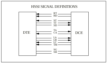
Signal Definitions
RT: Receive Timing from DCE
RT is a gapped clock with a maximum bit rate of 52 Mbps, and provides receive signal element timing information for RD.
RD: Receive Data from DCE
The data signals generated by the DCE, in response to data channel line signals received from a remote data station, are transferred on this circuit to the DTE. RD is synchronous with RT.
ST: Send Timing from DCE
ST is a gapped clock with a maximum bit rate of 52 Mbps, and provides transmit signal element timing information to the DTE.
TT: Terminal Timing to DCE
TT provides transmit signal element timing information to the DCE. TT is the ST signal echoed back to the DCE by the DTE. TT should be buffered by the DTE only, and not gated with any other signal.
SD: Send Data to DCE
The data signals originated by the DTE, to be transmitted via the data channel to a far end data station. SD is synchronous with TT.
TA: data Terminal equipment Available to DCE
TA will be asserted by the DTE, independently of CA, when the DTE is prepared to both send and receive data to and from the DCE. Valid data transmission should not commence until CA has also been asserted by the DCE. If the data communications channel requires a keep alive data pattern when the DTE is disconnected, then the DCE shall supply this pattern while TA is deasserted.
CA: data Communications equipment Available from DCE
CA will be asserted by the DCE, independently of TA, when the DCE is prepared to both send and receive data to and from the DTE. This indicates that the DCE has obtained a valid data communications channel. Data transmission should not commence until TA has also been asserted by the DTE.
Given that the data communications channel is not valid unless both TA and CA are asserted, then it may be good implementation practice to gate the incoming data stream with both TA and CA on both the DTE and the DCE.
It should also be recognized that when CA is deasserted by the DCE, the DCE is in an unknown state, and that ST and RT clocks may be absent and cannot be considered by the DTE as valid.
LA: Loopback circuit A to DCE
LB: Loopback circuit B to DCE
LA and LB are asserted by the DTE to cause the DCE and its associated data communications channel to provide one of three diagnostic loopback modes. Specifically, LB = 0, LA = 0: no loopback LB = 1, LA = 1: local DTE loopback LB = 0, LA = 1: local line loopback LB = 1, LA = 0: remote line loopback
A 1 represents assertion, and a 0 represents deassertion. All loopbacks are payload loopbacks. Therefore, if the HSSI data stream is multiplexed on to only part of the data communications channel, then, as a minimum, only that part of the data communications channel needs to be loopbacked.
A local DTE (?digital?) loopback occurs at the DTE port of the DCE, and is used to test the link between the DTE and DCE. A local line (?analog?) loopback occurs at the line side port of the DCE, and is used to test the DCE functionality. A remote line (?analog?) loopback occurs at the line port of the remote DCE, and is used to test the functionality of the data communications channel. These three loopbacks are initiated in this sequence. The remote DCE is tested by remotely commanding its local loopbacks. Note that LA and LB are direct supersets of the EIA signals LL (Local Loopback) and RL (Remote Loopback).
The local DCE continues to assert CA during all three loopback modes. If the local DCE is unable to support a particular loopback mode, then it may elect to deassert CA while LA or LB are asserted by the DTE, The remote DCE will deassert CA when remote loopback is in effect. If the remote DCE can detect a local loopback at the local DCE, then the remote DCE will deassert its CA; otherwise the remote DCE will assert its CA when there is a local loopback at the local DCE.
The DCE implements the loopback towards the commanding DTE only. Receive data from the data communications channel is ignored. Send data to the data communications channel is filled with either the commanding DTE?s send data stream, or with a keep alive data pattern, depending upon the data communications channel?s specific requirements.
There is no explicit hardware status signal to indicate that the DCE has entered a loopback mode. The DTE waits for an appropriate amount of time after asserting LA and LB before assuming the loopback to be valid. The appropriate amount of time is application dependent, and is not a part of this specification.
The loopback mode applies to both timing and data signals. Thus, on the DTE -DCE link, the same timing signal could traverse the link three times, first as ST, then as TT, and finally as RT.
LC: Loopback circuit C from DCE
LC is an optional loopback request signal from the DCE to DTE, to request that the DTE provide a loopback path to the DCE. More specifically, the DTE would set TT=RT and SD=RD. ST would not be used, and could not be relied upon as a valid clock source under these circumstances.
This would then allow the DCE/DSU network management diagnostics to test the DCE/DTE interface independent of the DTE. This follows the HSSI philosophy that both the DCE and the DTE are intelligent independent peers, and that the DCE is capable of and responsible for maintaining its own data communications channel.
In the event that both the DTE and DCE asserted loopback requests, the DTE will be given preference.
Note that LC is optional and has not been included in the ANSI standard.
TM: Test Mode from DCE
Test Mode is asserted by the DCE when it is in a test mode caused by either local or remote loopbacks. This signal is optional. TM has been added by ANSI and was not part of the original HSSI specification.
SG: Signal Ground
SG is connect?s to circuit ground at both ends. SG ensures that the transmit signal levels stay within the common mode input range of the receivers.
SH: Shield Direction
The shield encapsulates the cable for EMI purposes, and is not implicitly intended to carry signal return currents. The shield is connected to DTE frame ground directly, and may choose one of two options at the DCE frame ground.
The first option is to connect the shield to DCE frame ground directly.
The second option is to connect the shield to DCE frameground through a parallel combination of a 470 ohm, +/-10%, 1/2 wattresistor, 0.1 uF, +/- 10%, 50 volt, monolithic ceramic capacitor, and a 0.01 uF, +/- 10%, 50 volt, monolithic ceramic capacitor.
The R-C-C network should be located as close to the shield/chassis junction as possible. Because the shield is terminated directly to the DTE and DCE chassis, the shield is not given a pin assignment within the connector. Shield continuity between connecting cables is maintained by the connector housing.
In practice, the first option is usually used.
Electrical Characteristics
All signals are balanced, differentially driven, and received at standard ECL levels. The ECL negative supply voltage, Vee, may be either -5.2 Vdc +/- 10% or -5.0 Vdc +/- 10% at either end. Rise times and fall times are measured from 20% to 80% threshold levels. Electrical characteristics of the HSSI transmitter and receiver are given in the HSSI Receiver table and the HSSI Transmitter table, both of which are presented below.
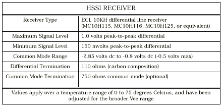
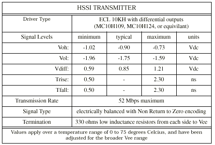
In addition to the 10KH ECL electrical characteristics listed in this specification, interoperation with 100K ECL is also possible and will be allowed for in the ANSI specification.
Fail Safe Operation
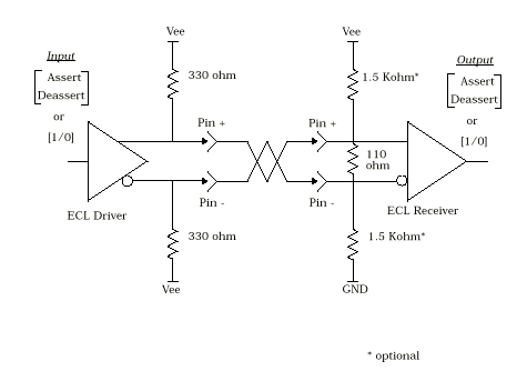
In the event that the interface cable is not present, the differential ECL receivers must default to a known state. To guarantee this, it is necessary when using the 10H115 or 10H116 to add a 1.5 kohm, 1%, pull-up resistor to the (-side) of the receiver, and a 1.5 kohm, 1%, pull-down resistor to the (+side) of the receiver.
This allows the proper 150 mvolts minimum to be developed across the 110 ohm resistors and will create a longitudinal termination of 750 ohms. The default state of all interface signals is deasserted.
It is not necessary to use external resistors when using the 10H125 since it has an internal bias network which will force an output low state when the inputs are left floating.
The interface must not be damaged by an open circuit or short circuit connection on any combination of pins.
Timing
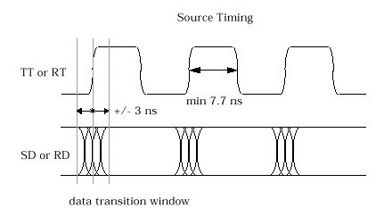
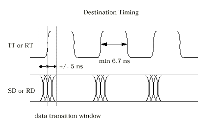
Source timing is defined as timing waveforms generated at a transmitter. Destination timing is defined as timing waveforms incident at a receiver. Pulse widths are measured between 50% points of the final pulse amplitude. The leading edge of the timing pulse shall be defined as the boundary between deassertion and assertion. The trailing edge of the timing pulse shall be defined as the boundary between assertion and deassertion.
The HSSI link, from a specification and implementation point of view, should be considered as a ECL flip-flop to flip-flop link. As data leaves the HSSI port, it should be reclocked out of an ECL flip flop and directly into the line driver. At the receiver, once passing through the line receiver, the data should immediately again be reclocked into an ECL flip flop. Control signals do not require the use of a flip-flop.
RT, TT, and ST minimum positive source timing pulse width shall be 7.7 ns. This allows a source duty cycle tolerance of +/- 10%. This value is obtained from:
10%         = ((9.61ns - 7.7ns)/19.23ns)
              x100%
where:
19.23 ns = 1 / (52 Mbps)


9.61 ns = 19.23 ns * 1/2 cycle
Data will change to its new state within +/- 3 ns of the leading edge of the source timing pulse.
RT, TT, and ST minimum positive destination timing pulse width shall be 6.7 ns. Data will change to its new state within +/- 5 ns of the leading edge of the destination timing pulse. These numbers allow for transmission distortion elements of 1.0 ns of pulse width distortion and 2.0 ns of clock to data skew. This leaves 1.7 ns for receiver setup time.
The data will be considered valid on the trailing edge. Thus, transmitters clock data out on the leading edge, and receivers clock data in on the trailing edge. This allows an acceptance window for clock-data skew error.
The delay from the ST port to the TT port within the DTE shall be less than 50 ns. The DCE must be able to tolerate a delay of at least 200 ns between its ST port and its TT port. This allows for a 150 ns delay for 15 meters of cable (round trip delay)
To facilitate various bit/byte/frame DCE multiplexor implementations, RT and ST may be gapped to allow the deletion of framing pulses and to allow bandwidth limiting of the HSSI.
The maximum gapping interval is not specified. However, the clock sources ST and RT are expected to be generally continuous when both TA and CA are asserted. A gapping interval is measured as the amount of time between two consecutive clock edges of the same slope.
The instantaneous data transfer rate must never exceed 52 Mbps.
The definition of valid data is application dependent and not a subject of this specification. This is consistent with HSSI being a layer 1 specification, and therefore having no knowledge of data validity.
CA and TA are asynchronous of each other. Upon assertion of CA, the signals ST, RT, and RD will not be considered valid for at least 40 ns. Upon the assertion of TA, the signals TT and SD will not be considered valid for at least 40 ns. This is intended to allow the receiving end sufficient setup time.
TA should not be deasserted until at least one clock pulse after the last valid data bit on SD has been transmitted. This does not apply to CA since the data is transparent to the DCE.
Physical Specification
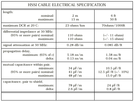
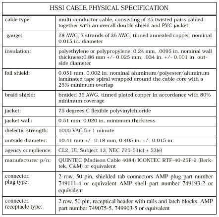
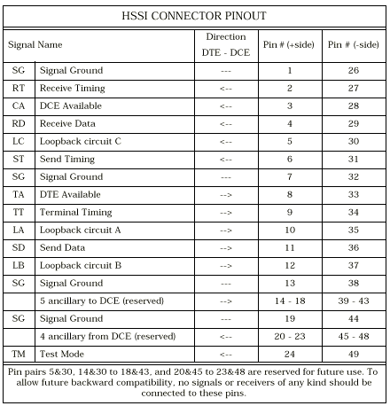
The cable connecting the DCE and DTE consists of 25 twisted pairs with an overall foil/braid shield. The cable connectors are both male connectors. The DTE and DCE have female receptacles. Dimensions are given in meters (m) and feet (ft).
Note that although the HSSI cable uses the same connector as the SCSI-2 specification, the cable impedances of HSSI and SCSI-2 cables are different. SCSI-2 cables can be as low as 70 ohms, whereas HSSI cables are specified at 110 ohms. As a result, cables made to SCSI-2 specifications may not work correctly with HSSI. Incompatibilities will be more apparent with longer lengths of cables.
The cable is completely described in the HSSI Cable Electrical Specification table, the HSSI Cable Physical Specification table, and the HSSI Connector Pinout table, all of which are presented below.
Appendix A: Timing Diagrams
Appendix B: Differential Circuit Conventions
Appendix C: Noise Immunity
This appendix calculates the noise immunity of this interface. The normal specified 150 mvolts of noise immunity for 10KH ECL is not applicable here because the differential inputs do not use the internal ECL bias Vbb.
The common mode (NMcm) and differential mode (NMdiff) noise margins for the 10H115 and 10H116 differential line receivers are:
NMcm+ = Vcm_max - Voh_max

      = -0.50 Vdc - (-0.81 Vdc)

      = 310 mVdc


NMcm- = Vol_min - Vcm_min

      = -1.95 Vdc - (-2.85 Vdc)

      = 900 mVdc


NMdiff = Vod_min * length

       * attenuation/length

       - Vid_min

       = 590 mv

       /[10^((50 ft *.085 dB/ft)/20)]

       - 150 mv

       = 361 mv


in dB:

       = 20 log [(361+150)/150]

       = 10.6 dB
Voltages are at 25 degrees Celsius. Vcm_max was chosen to be 100 mv below the saturation point of Vih = -0.4 volts.
The 10H125 differential receiver has a +5 Vdc supply and can handle a larger positive excursion on its input. The noise margin performance of the 10H125 is:
NMcm+ = Vcm_max - Voh_max

      = 1.19 Vdc - (-0.81 Vdc)

      = 2000 mVdc
NMcm- and NMdiff are the same for all parts. To allow the use of all receivers, the worst case common mode noise at the receiver must be limited to 310 mvdc.
Interpret the common mode range, Vcm_max to Vcm_min, as the maximum range of absolute voltages that may be applied to the receiver?s input, independent of the applied differential voltage. The signal voltage range, Voh_max to Vol_min, represents the maximum range of absolute voltages that the transmitter will produce. The difference between these two ranges represents the common mode noise margins, NMcm+ and NMcm-, with NMcm+ being the maximum excursion for additive common mode noise, and NMcm- being the maximum excursion for subtractive common mode noise.
With five 50 foot twisted pair grounds, the amount of ground loop current required to use up the common mode noise margin is:
I_ground = NMcm+

         / (cable_resistance/5 pairs)

         = (310 mVdc)

         / (70 mohms/foot

         x 50 feet / 10 wires)

         = 0.9 amps dc
This amount of current should never be present under normal operating conditions.
Common mode noise will have a negligible effect on the differential noise margin, Vdf_app. Rather, Vdf_app would be affected by noise being introduced by one side of the power rails at the transmitter. ECL Vcc has a power supply rejection ratio (PSRR) of 0 dB while ECL Vee has a PSRR on the order of 38 dB. Thus, to minimize differential noise, Vcc is grounded and Vee is connected to a negative power supply.
 Feedback