BITS Wiring Information and Looped BITS Timing on ONS 15454
Available Languages
Contents
Introduction
This document describes Building Integrated Timing Supply (BITS) wiring information and presents a case for looped BITS timing configuration on Cisco ONS 15454.
Prerequisites
Requirements
Cisco recommends that you have knowledge of these topics:
-
Cisco ONS 15454
-
GR Core Telecordia Standards
Components Used
The information in this document is based on these software and hardware versions:
-
Cisco ONS 15454
The information in this document was created from the devices in a specific lab environment. All of the devices used in this document started with a cleared (default) configuration. If your network is live, make sure that you understand the potential impact of any command.
Conventions
Refer to Cisco Technical Tips Conventions for more information on document conventions.
BITS Wiring Information
Each ANSI chassis has two incoming BITS (1 and 2) ports and two outgoing BITS (1 and 2) ports. Two pins are assigned for each clock signal as shown in Table 1.
Table 1 – BITS Wiring Chart| External Device | Function | Contact | Tip or Ring |
|---|---|---|---|
| BITS 1 | Out | A3 | Ring |
| Out | B3 | Tip | |
| In | A4 | Ring | |
| In | B4 | Tip | |
| BITS 2 | Out | A1 | Ring |
| Out | B1 | Tip | |
| In | A2 | Ring | |
| In | B2 | Tip |
A standard T1/E1 connector contains 8 pins with 4 wires (1, 2, 4 and 5) active. The device type (DCE or DTE) defines T1 pins as shown in Table 2.
Table 2 – T1 Pin Out| Pin # | Name | DCE (Network) | DTE (Customer) |
|---|---|---|---|
| 1 | R | Tx Ring | Rx Ring |
| 2 | T | Tx Tip | Rx Tip |
| 4 | R1 | Rx Ring | Tx Ring |
| 5 | T1 | Rx Tip | Tx Tip |
Note: Here is the key to the terms in Table 2:
-
Tx: Transmits out of a terminating device.
-
Rx: Receives in to a terminating device.
-
Tip: Positive (+).
-
Ring: Negative (-).
When you connect a DCE to a DTE (a typical configuration), you must use a straight through cable. Otherwise you need a cross-over cable. For example, you need a cross-over cable to connect a DTE to another DTE, so that a Tx Tip communicates with an Rx Tip, and a Tx Ring communicates with an Rx Ring. In such a cable, pin 1 of one connector always terminates on pin 4 of the other connector, and pin 2 of one connector always terminates on pin 5 of the other connector.
Cisco recommends 100-ohm type #22 or #24 AWG shielded twisted pair cable. Category 5 shielded twisted pair cables meet this criterion. Use solid conductors for tight wrapping. Also, provision line build out correctly to minimize cable-related issues.
RJ-48C and RC-45 are two common connectors that you can use for T1 termination. Both have eight pins.
Timing T1/E1 connections involve simplex data, which refers to one-way communication from timing source to receiver. Therefore, you require only two wires for each timing signal. In order to ensure that the port does not go down, the provider can provision an internal loopback for the port. In order to connect BITS clock to BITS In pins, connect ring to ring and tip to tip. For example, for BITS1 In, you must wire pin 1 to A4 and pin 2 to B4.
For the ETSI chassis, four miniature coaxial connectors provide two inputs and two outputs. You can find them in slot 24 MIC-C/T/P card on FMEC. The top two connectors are for BITS 1 (In on the left and Out on the right) and the bottom two connectors are for BITS 2 (In on the left and Out on the right). The cable is a 75-ohm coaxial cable with a 1.0/2.3 miniature coaxial connector.
Looped BITS Timing
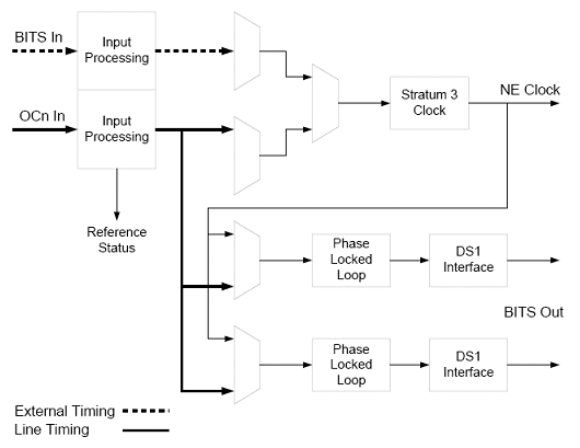
A Mixed timing mode uses both external and line inputs as references. The danger with Mixed timing is the potential for timing loops. As an alternative to Mixed timing, you can use the BITS output that you derive from an optical line as an input to a secondary BITS. There are several ways to wire and provision the looped BITS timing (see Figure 1 for an example).
Figure 1 – ONS 15454 Timing Circuit 
Note: The use of looped BITS configuration does not prevent timing loops. Use the same caution as with the Mixed mode provisioning.
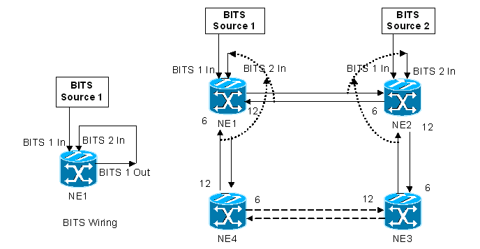
Wire one of the two BITS Out (BITS 1 Out) directly to the second BITS In pins (see Figure 2).
Figure 2 – A Sample Looped BITS Configuration 
Wire pin A3 is to pin A2 and pin B3 is to pin B2. Wire BITS 1 In as discussed previously.
Provision BITS 2 In as a second external reference, in addition to the BITS from the attached BITS device (the primary reference). Similarly, wire and provision both NE1 and NE2.
NE4 derives the primary timing from NE1, and secondary timing from NE3. NE3 derives the primary timing from NE2, and secondary timing from NE4. Enable Source Specific Multicast (SSM) on all nodes.
In order to activate BITS Out, provision two lines as the timing sources for BITS 1 Out. On NE1, a port on slot 12 is the primary source and a port on slot 6 is the secondary source. On NE2, slot 6 is the primary source and slot 12 is the secondary source.
Table 3 shows the timing provisioning information for all four nodes.
Table 3 – Timing Provisioning Information| Device | Timing Mode | Primary | Secondary | Third | BITS 1 Out Primary | BITS 1 Out Secondary |
|---|---|---|---|---|---|---|
| NE1 | External | BITS 1 In | BITS 2 In | Internal | 12 | 6 |
| NE2 | External | BITS 1 In | BITS 2 In | Internal | 6 | 12 |
| NE3 | Line | 6 | 12 | Internal | - | - |
| NE4 | Line | 12 | 6 | Internal | - | - |
You can analyze at least three failure scenarios for this timing scheme, as explained here:
-
Scenario 1: BITS Source 1 fails
When BITS Source 1 fails, NE1 switches to BITS 2, which is derived from slot 12 and thus from BITS Source 2. There is no timing switch on any other nodes.
-
Scenario 2: Both BITS Source 1 and BITS Source 2 fail
When BITS Source 2 also fails after BITS Source 1 failure, NE2 enters the Holdover mode, because NE2 receives DUS from slots 6 and 12. All four nodes are timed from the internal oscillator of NE2.
-
Scenario 3: BITS Source 1 and the link between NE1 and NE2 fail
When BITS Source 1 fails and the link between NE1 and NE2 fails thereafter, NE1 enters the Holdover mode because NE1 receives DUS from slot 6. NE4 switches to the secondary source from NE3, and removes the DUS that NE1 receives. Therefore, NE1 is able to switch to BITS 2 In.
Related Information
Contact Cisco
- Open a Support Case

- (Requires a Cisco Service Contract)
 Feedback