Power and I/O Signals at the ESR BTB Connector

This chapter contains the following sections:

Power and I/O Signals at the ESR BTB Connector

This section contains tables describing the control signals for different components. In the following tables, you will see the terms PU and PD. These stand for:

  • PU = Pull-Up resistor
  • PD = Pull-Down resistor

Note


Differential pairs should be mostly routed on inner layers where the impedance tolerance is controlled better. Outer layers should only be used for very short differential pair traces (less than 0.25").

Power Signals

Signal Name

Direction

Terminations

Description

Levels

+5V

IN

+5V Power Input to ESR board

5V DC

+3.3V

IN

+3.3V Power Input to ESR board

3.3V DC

RTC_3.0V

IN

Series 1K resistor required at Host

Note 6

+3.0V RTC Battery Power Input to ESR board

3.0V DC

GND

Ground

GND

+1.8V_OUT

OUT

+1.8V output from ESR board

Caution

 
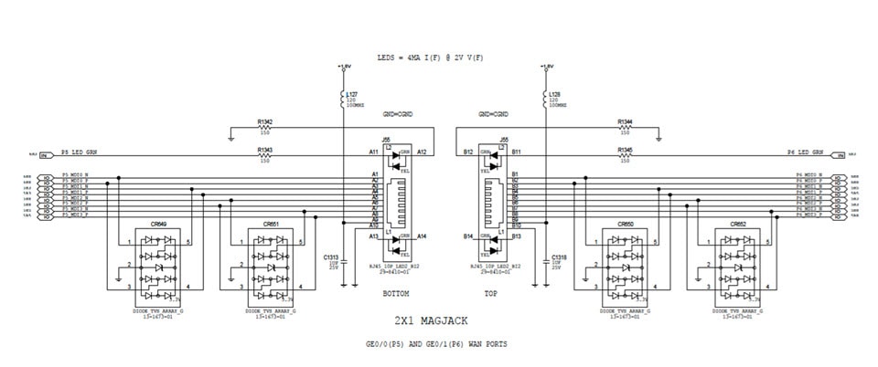
1.8V source is only intended for use as a WAN port center tap voltage as shown in the reference design schematic. 50mA is the max that can be drawn from that 1.8V output.

See EVK Schematics below for further detail.

1.8V DC

P3V3_TRIM

Trim signal to margin 3.3V +/-5%

See reference design schematic for proper usage.

(For test purposes only. Leave unconnected if not used.)

Passive

DCIN_PWR_GOOD

Note 8

IN

50K PU at ESR

Note 1

External Power Supply Status Detect input (3.3V digital signal at the ESR connector).

Can be used as an early power failure detect of the main power source.

Active High (0 = Power Supply status is not good. 1 = Power Supply status is good.)

3.3V CMOS

Note 1 : Signal driver can be open drain with a strong pullup (4.7K to 10K), or can be driven by 3.3V push-pull levels. A pull-down is not allowed on this signal. Can be left unconnected if not used.

Note 6 : Series 1K current-limiting resistor is required on the host board for the RTC 3.0V battery.

Note 8 : (currently not supported by software for graceful shutdown, but could be in the future). Used for successful CPU power up and boot. Must be driven or pulled high at powerup, or left open (because it is already pulled up by the ESR and keeps it in a “good” state for proper power up and CPU boot if left open).

Figure 1. EVK Schematic

LED Control Signals

Signal Name Direction Terminations Description Levels

SYS_LED_GRN_L

OUT

10K PD at ESR

Note 3

270 Ohm series resistor at Host.

Note 7

System Green LED Enable (active low)

3.3V CMOS

SYS_LED_YEL_L

OUT

10K PD at ESR

Note 3

270 Ohm series resistor at Host.

Note 7

System Yellow LED Enable (active low)

3.3V CMOS

ALM_LED_RED

OUT

1K PD at ESR

Note 3

270 Ohm series resistor at Host.

Note 7

Alarm Red LED Enable (active high)

3.3V CMOS

VPN_LED_GRN

OUT

4.7K PU at ESR

Note 3

270 Ohm series resistor at Host.

Note 7

VPN Green LED Enable (active high)

3.3V CMOS

R0_LED

OUT

270 Ohm series resistor at Host.

Note 7

Row 0 LED control for LAN Ports GE 1/1 and GE 1/0.

(controls cathode-side of 2 single-color LEDs).

Cathode-side LED Enable (driven by Ethernet Switch on ESR) - Active Low.

Tie to Cathode side of two single-color Green LEDs through a resistor to each (e.g., 270 ohms for a 5mA forward current on each of the 2 LEDs).

3.3V CMOS

C0_LED

OUT

4.7K PD at ESR

Note 3

Column 0 LED control for LAN Ports GE 1/2 and GE 1/0.

(controls anode-side of 2 single-color LEDs).

(Anode-side LED Enable (driven by Ethernet Switch on ESR) - Active high.

Tie DIRECTLY to Anode side of two single-color Green LEDs.

3.3V CMOS

R1_LED OUT

270 Ohm series resistor at Host.

Note 7

Row 1 LED control for LAN Ports GE 1/3 and GE 1/2 .

(controls cathode-side of 2 single-color LEDs).

Cathode-side LED Enable (driven by Ethernet Switch on ESR) - Active Low.

Tie to Cathode side of two single-color Green LEDs through a resistor to each (for example, 270 ohms for a 5mA forward current on each of the 2 LEDs).

3.3V CMOS
C1_LED OUT

4.7K PD at ESR

Note 3

Column 1 LED control for LAN Ports GE 1/3 and GE 1/1.

(controls anode-side of 2 single-color LEDs).

(Anode-side LED Enable (driven by Ethernet Switch on ESR) - Active high.

Tie DIRECTLY to Anode side of two single-color Green LEDs.

3.3V CMOS
P5_LED_GRN OUT

270 Ohm series resistor at Host.

Note 7

WAN Copper Port (GE 0/0) LED Enable (controlled by Ethernet PHY on ESR) - Active High 3.3V CMOS
SFP1_LED_YEL OUT

270 Ohm series resistor at Host.

Note 7

WAN SFP Port (SFP 0/0) LED Enable (controlled by Ethernet PHY on ESR) - Active High 3.3V CMOS
P6_LED_GRN OUT

270 Ohm series resistor at Host.

Note 7

WAN Copper Port (GE 0/1) LED Enable (controlled by Ethernet PHY on ESR) - Active High 3.3V CMOS
SFP2_LED_YEL OUT

270 Ohm series resistor at Host.

Note 7

WAN SFP Port (SFP 0/1) LED Enable (controlled by Ethernet PHY on ESR) - Active High 3.3V CMOS

Note 3 : PU/PD to signals already exist on Cisco ESR, PIM, SFP, or SSD modules. No need to add any more. If you do add redundant parallel PU/PD, it should be weak (10K to 100K). Do not add a strong PU/PD for the purpose of overriding it to the opposite state. Some existing ESR PUs and PDs set the default configuration of the ESR CPU and should not be changed, as they are necessary during system reset to configure bootup settings. However, after any system reset (after system boots up), those signals are free to be driven and free to change states.

Note 7 : Series current-limiting resistor is required on host board for the LED driving signals. LEDs on host board should be chosen so that they operate well at 5mA forward current.

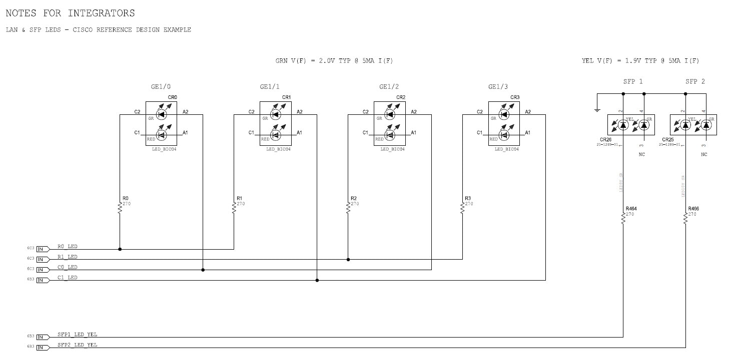
See the following figure for a design reference.

Figure 2. LAN and SFP LED Reference Design

Note


The Marvell Ethernet PHY chip set controls the LEDs, simply implement as shown in the reference design schematics. The Marvell chip minimizes the number of control lines by row and column to convey the correct link state and activity indication for all 4 ports. Cisco software does not control the ethernet port LEDs directly.

Gigabit Ethernet Port Signals

Signal Name

Direction

Terminations

Description

Levels

Impedance

SFP_2_TXD_[ P/N ]

OUT

Series Caps at SFP

Note 2

Port 6 (WAN SFP 0/1) SFP Transmit Differential Pair

1.6V Max LVDS

100 Ohm Differential

+/-10% (inner layers)

+/-15% (outer layers

SFP_2_RXD_[ P/N ]

IN

Series Caps at SFP

Note 2

Port 6 (WAN SFP 0/1) SFP Receive Differential Pair

2.1V Max LVDS

100 Ohm Differential

+/-10% (inner layers)

+/-15% (outer layers

SFP_1_TXD_[ P/N ]

OUT

Series Caps at SFP

Note 2

Port 5 (WAN SFP 0/0) SFP Transmit Differential Pair

1.6V Max LVDS

100 Ohm Differential

+/-10% (inner layers)

+/-15% (outer layers

SFP_1_RXD_[ P/N ]

IN

Series Caps at SFP

Note 2

Port 5 (WAN SFP 0/0) SFP Receive Differential Pair

2.1V Max LVDS

100 Ohm Differential

+/-10% (inner layers)

+/-15% (outer layers

P6_MDI[3..0]_[ P/N ]

BI

Port 6 (WAN GE 0/1) MDI Differential Pairs for 10/100/1000 Gigabit Ethernet Copper Ports

2.8V Max MDI

100 Ohm Differential

+/-10% (inner layers)

+/-15% (outer layers

P5_MDI[3..0]_[ P/N ]

BI

Port 5 (WAN GE 0/0) MDI Differential Pairs for 10/100/1000 Gigabit Ethernet Copper Ports

2.8V Max MDI

100 Ohm Differential

+/-10% (inner layers)

+/-15% (outer layers

P4_MDI[3..0]_[ P/N ]

BI

Port 4 (LAN GE 1/3) MDI Differential Pairs for 10/100/1000 Gigabit Ethernet Copper Ports

1.4V Max MDI

100 Ohm Differential

+/-10% (inner layers)

+/-15% (outer layers

P3_MDI[3..0]_[ P/N ]

BI

Port 3 (LAN GE 1/2) MDI Differential Pairs for 10/100/1000 Gigabit Ethernet Copper Ports

1.4V Max MDI

100 Ohm Differential

+/-10% (inner layers)

+/-15% (outer layers

P2_MDI[3..0]_[ P/N ]

BI

Port 2 (LAN GE 1/1) MDI Differential Pairs for 10/100/1000 Gigabit Ethernet Copper Ports

1.4V Max MDI

100 Ohm Differential

+/-10% (inner layers)

+/-15% (outer layers

P1_MDI[3..0]_[ P/N ]

BI

Port 1 (LAN GE 1/0) MDI Differential Pairs for 10/100/1000 Gigabit Ethernet Copper Ports

1.4V Max MDI

100 Ohm Differential

+/-10% (inner layers)

+/-15% (outer layers

Note 2 : Series AC-coupling caps to SERDES signals already exist on Cisco ESR, PIM or SFP module. No need to add any more.

Module Interface Signals

Signal Name Direction Terminations Description Levels Impedance

PCIE_REFCLK_[ P/N ]

OUT

If not used, keep open. The router will disable the PCIE reference clock when no PCIe is present.

PCIe 100MHz Differential Pair Reference Clock for Pluggable or SSD Module

1.6V Max LVDS

100 Ohm Differential

+/-10% (inner layers)

+-15% (outer layers

PIM_SGMII_TX_[ P/N ]

OUT

Series Caps at PIM

Note 2

SGMII Transmit Differential Pair for Pluggable Module (Can be PCIe TX also)

1.6V Max LVDS

100 Ohm Differential

+/-10% (inner layers)

+-15% (outer layers

PIM_SGMII_RX_[ P/N ]

IN

Series Caps at ESR

Note 2

SGMII Receive Differential Pair for Pluggable Module (Can be PCIe RX also)

1.6V Max LVDS

100 Ohm Differential

+/-10% (inner layers)

+-15% (outer layers

PIM_USB3_TX_[ P/N ]

OUT

Series Caps at ESR

Note 2

USB 3.0 Transmit Differential Pair for Pluggable Module

1.2V Max USB

90 Ohm Differential

+/-10% (inner layers)

+-15% (outer layers

PIM_USB3_RX_[ P/N ]

IN

Series Caps at PIM

Note 2

USB 3.0 Receive Differential Pair for Pluggable Module

1.2V Max USB

90 Ohm Differential

+/-10% (inner layers)

+-15% (outer layers

PIM_USB2_[ DP/DN ]

BI

2x 15K PD at ESR

USB 2.0 Differential Pair for Pluggable Module

3.6V Max USB

90 Ohm Differential

+/-10% (inner layers)

+-15% (outer layers

PIM_UA2_TXD

OUT

10K PU at PIM

Note 3

UART2 Transmit Data for Pluggable Module

3.3V CMOS

50 Ohm Single-Ended

+/-10% (inner layers)

+-15% (outer layers

PIM_UA2_RXD

IN

4.7K PU at ESR

Note 3

UART2 Receive Data for Pluggable Module

3.3V CMOS

50 Ohm Single-Ended

+/-10% (inner layers)

+-15% (outer layers

SSD_TX_SERDES_[ P/N ]

OUT

Series Caps at Host

Note 4

SERDES Transmit Differential Pair for SSD Module (Can be SATA or PCIe)

1.6V Max LVDS

100 Ohm Differential

+/-10% (inner layers)

+-15% (outer layers

SSD_RX_SERDES_[ P/N ]

IN

Series Caps at ESR

Note 2

SERDES Receive Differential Pair for SSD Module (Can be SATA or PCIe)

1.6V Max LVDS

100 Ohm Differential

+/-10% (inner layers)

+-15% (outer layers

PIM_PWR_EN

OUT

1K PD at PIM

Note 3

Power Enable signal for the Pluggable Module.

Active high (0 = disable Pluggable power. 1 = Enable Pluggable power.)

3.3V CMOS

PIM_GPS

IN

4.7K PU at ESRIf not used, keep open. The router will pull it up and keep it in an idle state.

Note 3

GPS Pulse Per Second Timing signal from Pluggable Module

3.3V CMOS

50 Ohm Single-Ended

+/-10% (inner layers)

+-15% (outer layers

Note 2 : Series AC-coupling caps to SERDES signals already exist on Cisco ESR, PIM or SFP module. No need to add any more.

Note 3 : PU/PD to signals already exist on Cisco ESR, PIM, SFP, or SSD modules. No need to add any more. If you do add redundant parallel PU/PD, it should be weak (10K to 100K). Do not add a strong PU/PD for the purpose of overriding it to the opposite state. Some existing ESR PUs and PDs set the default configuration of the ESR CPU and should not be changed.

Note 4 : Series caps required on the host board for these SERDES signals.

External Port Signals

Signal Name

Direction

Terminations

Description

Levels

Impedance

USB3A_TX_[ P/N ]

OUT

Series Caps at ESR

Note 2

USB 3.0 Transmit Differential Pair for External USB Host Port

1.2V Max USB

90 Ohm Differential

+/-10% (inner layers)

+-15% (outer layers

USB3A_RX_[ P/N ]

IN

Series Caps at Host

Note 4

USB 3.0 Receive Differential Pair for External USB Host Port

1.2V Max USB

90 Ohm Differential

+/-10% (inner layers)

+-15% (outer layers

USBA_[ DP/DN ]

BI

2x 15K PD at ESR

USB 2.0 Differential Pair for External USB Host Port

3.6V Max USB

90 Ohm Differential

+/-10% (inner layers)

+-15% (outer layers

USBA_5V_EN

OUT

1K PD at ESR

Note 3

Enable 5V output of the external USB Host Port.

Active High (0 = disable 5V USB output. 1 = enable USB 5V output)

3.3V CMOS

USBA_OC_L

IN

10K PU at Host

Note 5

Over Current Detect of the external USB Host Port.

Active Low (0 = USB host port 5V is in overcurrent condition. 1 = Normal Operation)

3.3V CMOS

CP_UA0_DTR

OUT

10K PU at Host

Note 5

UART0 DTR flow control signal for external RS232 Serial Port

3.3V CMOS

50 Ohm Single-Ended

+/-10% (inner layers)

+/-15% (outer layers

CP_UA0_DSR

IN

4.7K PU at ESR

Note 3

UART0 DSR flow control signal for external RS232 Serial Port

3.3V CMOS

50 Ohm Single-Ended

+/-10% (inner layers)

+/-15% (outer layers

CP_UA0_RTS

OUT

10K PU at Host

Note 5

UART0 RTS flow control signal for external RS232 Serial Port

3.3V CMOS

50 Ohm Single-Ended

+/-10% (inner layers)

+/-15% (outer layers

CP_UA0_CTS

IN

4.7K PU at ESR

Note 3

UART0 CTS flow control signal for external RS232 Serial Port

3.3V CMOS

50 Ohm Single-Ended

+/-10% (inner layers)

+/-15% (outer layers

CP_UA0_TXD

OUT

10K PU at Host

Note 5

UART0 Transmit Data for external RS232 Serial Port

3.3V CMOS

50 Ohm Single-Ended

+/-10% (inner layers)

+/-15% (outer layers

CP_UA0_RXD

IN

4.7K PU at ESR

Note 3

UART0 Receive Data for external RS232 Serial Port

3.3V CMOS

50 Ohm Single-Ended

+/-10% (inner layers)

+/-15% (outer layers

AP_UA0_TXD

OUT

1K PD at ESR

Note 3

Transmit Data for Console Port

3.3V CMOS

50 Ohm Single-Ended

+/-10% (inner layers)

+/-15% (outer layers

AP_UA0_RXD

IN

100K PU at Host

Note 5

Receive Data for Console Port

3.3V CMOS

50 Ohm Single-Ended

+/-10% (inner layers)

+/-15% (outer layers

ALM_IN_L

IN

4.7K PU at ESRIf not used, keep open. The router will pull it up and keep it in an idle state.

Note 3

Alarm Input (3.3V digital signal at the ESR connector).

Active Low (0 = external alarm port is closed. 1 = external alarm port is open circuit)

3.3V CMOS

PUSHBUTTON_L

IN

4.7K PU at ESRIf not used, keep open. The router will pull it up and keep it in an idle state.

Note 3

Pushbutton Detect Input (3.3V digital signal at the ESR connector).

Active Low (0 = pushbutton is closed. 1 = pushbutton is open).

3.3V CMOS

Note 2 : Series AC-coupling caps to SERDES signals already exist on Cisco ESR, PIM or SFP module. No need to add any more.

Note 3 : PU/PD to signals already exist on Cisco ESR, PIM, SFP, or SSD modules. No need to add any more. If you do add redundant parallel PU/PD, it should be weak (10K to 100K). Do not add a strong PU/PD for the purpose of overriding it to the opposite state. Some existing ESR PUs and PDs set the default configuration of the ESR CPU and should not be changed.

Note 4 : Series caps required on the host board for these SERDES signals.

Note 5 : PU/PD are required on the host board for these signals.

Miscellaneous Control Signals

Signal Name

Direction

Terminations

Description

Levels

Impedance

EVK_INT_L

IN

4.7K PU at ESR

Note 3

Reserved for Interrupt input to the ESR CPU from the host board. Currently not used by the Cisco Software to detect interrupts from the host motherboard. User should leave this signal unconnected, as the ESR provides the pullup.

3.3V CMOS

I2C2_SCL

OUT

4.7K PU at ESR

Note 3

Output Clock for I2C bus #2 to host board

3.3V CMOS

50 Ohm Single-Ended

+/-10% (inner layers)

+/-15% (outer layers

I2C2_SDA

BI

4.7K PU at ESR

Note 3

Bidirectional Data for I2C bus #2 to host board

3.3V CMOS

50 Ohm Single-Ended

+/-10% (inner layers)

+/-15% (outer layers

I2C3_SCL

OUT

4.7K PU at ESR

Note 3

Output Clock for I2C bus #3 to host board

3.3V CMOS

50 Ohm Single-Ended

+/-10% (inner layers)

+/-15% (outer layers

I2C3_SDA

BI

4.7K PU at ESR

Note 3

Bidirectional Data for I2C bus #3 to host board

3.3V CMOS

50 Ohm Single-Ended

+/-10% (inner layers)

+/-15% (outer layers

Note 3 : PU/PD to signals already exist on Cisco ESR, PIM, SFP, or SSD modules. No need to add any more. If you do add redundant parallel PU/PD, it should be weak (10K to 100K). Do not add a strong PU/PD for the purpose of overriding it to the opposite state. Some existing ESR PUs and PDs set the default configuration of the ESR CPU and should not be changed.